Viser opslag med etiketten Microcomputer. Vis alle opslag

onsdag den 15. oktober 2014

New project!

So, the z80 system 2 project being on hold until i get a functioning EPROM burner, I've moved forward on another project: The COSMAC ELF.
Though I've made some hardware mods, it is functionally equivalent of the original ELF. My mods include: 

    - Changing the HEX display to binary LED's; way cheaper.
This mod was actually suggested in the original article.

          - Changed the two 4 bit 2101 RAM's for eight 1 bit 2102 ones.
I had them lying around and besides the "width" they're very similar. Furthermore, they're 1977 vintage - adds something to the design.

    - Sprung for another layout, not wirewrap 
Once again, I'm out of wrap wire, and I kinda wanted it to have more of a Altair 8800 / MIPS 8080 kinda look.

Here it is:

The 8 chips with dual round indents are the RAM.

I have redrawn the schematic into a more reader friendly form than the original, spreading it over 6 pages:
1) CPU and clock
2A) Original RAM
2B) My RAM
3) I/O logic
4) Display
5) Input
6) CPU control

Makes it much easier to debug and alter.

Anyway, so far, I've wired the processor control and power.
Buses are to come.

tirsdag den 30. september 2014

Diode matrix ROM for the Z80, or: How a silly, not-so optimized idea became a main design choice.

Ok, so the phase one hardware design for the z80 system B is almost done. Even started on expanding, but I would like to have it running first. But alas: having no EPROM's, and no burner for them, i had to think of something for a complete hardware test. So i decided to code three small program snips into a diode matrix ROM for it.

What a beauty! I've expanded the design (see last post) for 32 bytes, using 2 74154 4-16 decoders, and then feeding the lower 4 addresses into those. the next two addresses are fed to a 2-4 decoder, whose 1 and 2 output enables either chip 1 or 2.
The design of the diode matrix itself was a bit tricky. Most designs needs either multiple boards, or 3d arrays of wires, but eventually, i landed on having each trace (32 of them) for each line run all the length of the left half of the board. then, soldering tin/copper wire across the top of the board, and connecting those to the data lines, with pull ups. the result is rather neat, in its own right.
The bytes are read upwards, meaning that A0 is the lowest row, and so on. A diode indicates a 0, while a missing diode is 1. This is stupid, in terms of saving diodes, since 00 is used more often than FF, but yeah. Still needs some bytes, though, i ran out of diodes.


It should be able to mimic a 2716, or any device, really. I may need a tri-state buffer on DATA bus, and have the gate tied to /CS, to keep the bus floating from the pull ups. We'll see.

Once again, the sample programs are some counters and stuff i found on Donn Stewart's z80 page. I still haven't gotten around programming yet.

fredag den 5. september 2014

Historic PROM burner: The DATAIO model IX

So, i bought this some time ago, a really interesting artifact of computer/digital electronics history.

It is, as far as my research go, nothing less than the worlds first microprocessor controlled PROM burner!

Yup, that's it. Pretty good condition, except for one missing button cover on the EDIT. It can check memory, copy it, browse through addresses, and many other functions. It has a parallel Dsub25 connector on the back, for "remote operation" - whether that means having "slave" programmers for multiple chips, or the unit being able to be controlled by other systems. I haven't found ANY documentation on this; no manual, nothing. the only reference to it is a note on DATA IO's website, under a company history timeline.

On the same timeline, they state that model 19 is the first microprocessor controlled burner (with MC6800) - That is wrong, since this model is earlier, and IS controlled by a 6800, making THIS the first. Though, whether it's the worlds first or the company's, I really haven't the foggiest.

THE GUTS

The case is in fiberglass, and split color blue/white, and is mounted on a 8 mm aluminum bottom plate - really adds some weight.

The computer part, which is what we want, is mounted in a little rack system, with a backplane bus of chained card-edge connectors on ribbon cable. There are 4 boards, with those lovely "ears" for releasing them from the rack.

************************THE PROCESSOR BOARD************************


If that ain't retro, I don't know what is! The memory is shared over 4 chips - 2x 2708 1K EPROMs, the white ceramic with gold windowframe/legs! i had to cover them, i were afraid the flash of the camera could damage the memory, so the windows are covered with masking tape. The plastic DIP24 with the sticker must be system ROM, and the MC6810 is the typical RAM to go with the MC6800. This RAM, is probably system RAM, there must be a reason why the RAM is split on two boards - more on that later. The shiny can is the MC6871A - an oscillator / two phase clock for the 6800. Not much else, a little logic and some jumpers. Notice how the address range of the memory is labeled in the silk screen: C600-C7FF and so on. That's neat!

************************MEMORY BOARD************************ 


 This is the RAM board. Little more than 2 AM9131ADC 1024x4 SRAM chips - yes, Advanced Micro Devices, AMD. Apparently, This can be expanded, by the two empty sockets. The RAM IC's is in the purple/grey/gold packages - same as the 6800 itself. I believe this RAM is for holding the PROM code in memory.

************************ I/O ************************

The I/O is again, as far as i can tell, very much standard 6800 peripheral stuff:


The 24 pin DIP package is the MC6850 ACIA Asynchronous Communications Interface Adapter, acting as an UART. The 40 pin package is the MC6821 peripherals adapter, driving, by the looks of the bus, the header connector top left, which goes to the front panel. The smaller second card edge connector (right) goes to the DSUB 25 connector. And a baud rate switch for the ACIA - what would happen if you activated more than one?

The main programming cards and IC sockets are connected directly to the main system bus, and consists of a set of two chip specific cards: A digital, dealing with timing and such, and an analog, setting voltages. I have yet to find any references as to what PROM my system is set up for, but changing chip for this model of burner must be quite a challenge. The analog board also needed calibration.

There's much more, so I'll probably do a follow up, but this is a brief description (ha. BRIEF) of the microprocessor/computer based parts.     

torsdag den 4. september 2014

Z80 computer update

It ALMOST lives. I'm currently working on the IO interface, which is just some latches and buffer logic with two ports of 8 LEDS and 8 switches. This "terminal" is connected via rainbow ribbon to a socket on the IO board:
The board is yet to be wired, which will be done in the style of the memory board.

The system as of writing looks like this:


The card labeled "memory card" is the memory card, and likewise with the others. You probably guessed that, though. I haven't made/bought the PSU yet, so it is powered by a variable psu, adjusted with a DMM. The ribbon is supposed to go to an angled front plate.

lørdag den 30. august 2014

Memory circuit wired

This is the memory card for my Z80 system. It contains a single 8x2k SRAM, the 6116-2, one of my favorite SRAM's, because its name is a palindrome. A 2716 EPROM of same size (and pin compatible, by the way) is used as system ROM. Address decoding for chip select with a 74139. Memory decoding entirely after Donn Stewart's Z80 computer. A more refined point-to-point wiring technique than with the indicator card, and i think it's really neat! Maybe even more so than wire-wrap. 

Using the same wire to make little ties for the wire bundles. 
For this method, start by wiring power, then control logic, and THEN DATA and ADDRESS buses, as you see, they are the ones who takes up space. Make sure that the wires are approximately the right length to be routed, and then after soldering of a bundle, begin "neating" with wire ties, either free floating or though holes in the PCB. excess length can be huddled up at one end (here, at the connector).  

fredag den 29. august 2014

The indicator card done

The indicator card made, with a different construction technique, since i wanted to exercise different prototyping methods for digital hardware. Okay, okay; I ran out of wire wrap wire.

Thiss is 26 AWG wire, thicker than W-W. wire, but not much. Still so thin the insulation goes through the standard PCB holes. gives a good deal of strain relief, and allows for use as wire binders.

Not much more to tell about this:


The processor card

The processor card is basically just a z80 with buffered buses and some functions. A clean reset circuit, and two clocks are on board as well. A manual step clock, and a slow clock ( a couple of Hz). This board, the clock and reset in particular, is inspired by CPUville's homebrew z80 project. This also served as the inspiration for this project. 

This is the card. The red % button is the reset, and the toggle switch is the manual clock. the header matrix to the left of the processor is to select the clock via jumper, so you don't accidentally switch on two clocks at the same time. 
Wire color code: RED: When it was closest. BLUE: When that was closest. Power is mainly routed on the solder side.


Computer base and indicator card!

OK, so these come pretty close one after another, since i'm actually past these steps, but behind on making a blog about it.

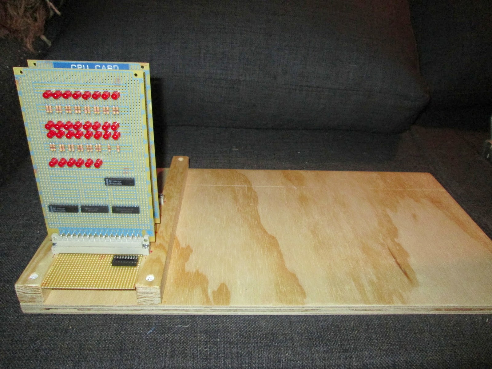
Well, the base is made, as mentioned from wood, and the Indicator card is made.
Well this is the indicator /bus display card. It is nothing fancy, just a binary readout of the entire bus. Upper row are DATA (7-0 in reading order), the two rows are ADDRESS(15-0), and the lower six are: Reset, Clock, Memrq, IOrq, RD and WR.
the four chips, 74LS241, is simply set up as noninverting buffers, which has some problems, since most of the control signals are active low. Good thing that won't confuse me when this machine doesn't do a thing!


Here be the base of the computer, the two cards installed. The dip socket on the bus card is to access the data bus, since i got the idea of wanting a little plug with pull-down resistors, to put the processor into free-run mode (just counting addresses, executing NOP's). Room is made for binary I/O, PSU, later: QWERTY keyboard, floppy drive, hard drive. 

Z80 microcomputer (SYSTEM B)

This is the progress on my Z80 computer project! I've recently received the needed components, and has begun construction.

The idea is, to make a eurocard (that's a PCB standard size) and backplane based microcomputer, which can be operated as simply as possible, but that also will allow for infinite expansions. 

Phase 1 consists on little more than a buffered CPU card with clock, and a bus display card, showing the logic level of the address and data bus as well as some control bus signals.

The "enclosure" is made of wood, to give that 70's homebrew feel, and the plan is not to use any component that didn't exist in the early to mid-80's.


Above can be seen the first card to be plugged into the backplane. The connectors are DIN 41617 connectors, because i like how the pins match up with regular stripboard. The card pcb's is IC-island types, FR4 material. The 4 20-pin packages are simply buffers for various busses.

I use a mix of prototyping techniques, here it's wire-wrap, though i use standard 0.1-inch header pins as wrap posts. This has two major advantages, 1) The card becomes very low-profile, with the height being about 1,5 cm instead of the almost 4 with ordinary wrap sockets. 2) each socket costs a fraction of a wire-wrap one. The connection might not be as good, though. I've yet to experience problems with that.